4. GMSL2-10GbE Conversion Module Hardware Reference Manual#
4.1. Overview#
The GMSL2-10GbE conversion module is an edge compute platform enabling low-latency data transfer from up to eight Gigabit Multimedia Serial Link™ (GMSL) interfaces to a host system via a 10Gb Ethernet link.
The system includes two MAX96724 Quad Tunneling GMSL2/1 to CSI-2 Deserializers, enabling connectivity of up to eight GMSL cameras. The video data from the cameras is fed via the MAX96724 MIPI-CSI2 interfaces to an AMD KV26 System-on-Module which implements the logic to aggregate the video data into a 10Gb Ethernet link to be sent to a central processing unit.
The IEEE1588 Precision Time Protocol (PTP) with hardware timestamping is supported, enabling accurate synchronization with host systems and other edge devices. The AD9545 Dual DPLL/IEEE1588, 1pps Synchronizer and Jitter Cleaner is used to generate the required clocks for the 10Gb Ethernet interface and the PTP logic.
16 general purpose I/O pins are available with software configurable functionality, operating at 3.3V voltage level.
A RS232 dedicated interface can be used to connect UART peripherals such as GNSS devices.
4.2. Mechanical specifications#
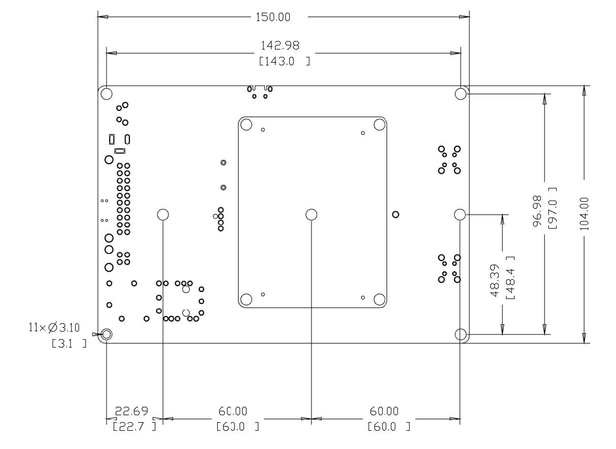
Fig. 4.14 Mechanical drawings#
4.3. Power and thermal#
Parameter |
Min |
Typ |
Max |
Unit |
Comments |
Supply voltage |
10 |
12 |
48 |
V |
Main power connector combined with I/O connector. 1 x Barrel jack power connector, can be used for main power or for the auxiliary power |
Power rating |
5 |
24 |
W |
Depends on system processing load |
|
Operating temperature |
-40 |
60 |
degC |
Measured at carrier PCB level. Proper cooling must be implemented to ensure operating temperature range |
4.4. Input / Output interface#
4.4.1. SFP+ Optical 10Gb Ethernet#
10Gb Ethernet MAC & PHY in FPGA
IEEE 1588 with hardware timestamping
SFP+ cage P/N : 2007194-1
SFP+ connector P/N : 1888247-1
4.4.2. UART (RS232)#
3.3V voltage level with current limit and overvoltage protection.
Functionalities:
Camera trigger / Flash signal x8
PPS output x1
PPS input x1
PWM output x1
I2C Connector P/N: 430452023
4.4.3. GPIO#
16 port, 3.3V voltage level with current limit and overvoltage protection Functionalities.
Camera trigger / Flash signal x8
PPS output x1
PPS input x1
PWM output x1
I2C
Connector P/N: 430452023
4.4.4. GMSL#
2 x HFM quad type mini-Fakra connector
Conector P/N: 2304168-9
4.4.5. SD Card#
Micro SD card holder, push to eject
4.4.6. USB2.0#
Console interface for Linux OS
4.4.7. JTAG#
Kria SoC PL Debug interface
4.5. Processing#
4.5.1. AMD Kria K26 SoM#
Industrial grade SoM (P/N: SM-K26-XCL2GI). Cooling solution not included
4.6. Firmware & Software#
4.6.1. Firmware#
Custom Linux image without desktop UI
Linux image update over Ethernet
Linux image stored in the Xilinx Kria SoM eMMC or on SD card
4.6.2. HTML User interface for system configuration and status#
Accessible over configurable IP address and port
Provides remote control for system configuration and status
RTP Control
Camera Trigger Settings
Streaming Settings
PTP Settings
Camera Settings
4.6.3. Remote system configuration and status via ssh#
ssh access into the system via the Ethernet interface
Provides access to all the system’s functions via the Linux standard drivers interfaces and tools
4.7. Synchronization#
4.7.1. IEEE1588#
Hardware timestamping
Configurable as slave or master
4.8. Camera control & data format#
4.8.1. Camera trigger control#
Each camera independently triggerable internally.
Using FSYNC + GPIO of deserializers for independent triggering of all four cameras on one deserializer
Internal triggering relative to system ToS
Each internal trigger configurable for frequency, phase, and duty cycle: 1Hz to 200Hz
External GPIO configured as output can be controlled in the same way as internal camera triggers
External GPIO configured as input can trigger the individual cameras directly
Trigger jitter at sub ms level
Trigger delay can also be configured (phase setting + delay to compensate for different camera triggering and exposure peculiarities)
4.8.2. Data timestamping#
Video packets packets timestamped with PTP-synchronized system time. Timestamp format options:
32bit NTP
96bit PTP
Images timestamps generated at trigger (FSYNC), end of frame or start of frame, using FPGA timestamping (PTP -synchronized system time)
Configurable timestamp offset
4.8.3. Video data format#
UDP data output
RTP compliant as per RFC3550 & RFC4175